Last week I wrote my 555 contest entry on 555-logic (and its 2-bit grey-code counter implementation as proof of concept) on this blog in a huge rush. As my wife was waiting for me to accompany her for some business, I had to finish up the 555 contest entry report which was due only a few hours before deadline (due to geographical location advantage, I get to sleep at midnight and rush afterwards, in the morning instead :D)
I started the idea to make 555-based digital logic circuits quite early when time was plenty before the 555 contest submission deadline. Another crazy idea in my mind was actually to make an Op Amp out of a 555. Last semester I taught analog electronics, and one of the lab experiment in the class was to actually build a self-made op amp with those very popular 9012s and 9013 BJTs in Indonesia. But it didn’t take long before I scrapped this idea, thinking it was kind of almost impossible, since not all comparator pins (it has this similar symbol with an op amp right?) inside the 555 could be accessed. I once read a PhD thesis that had this VCO-based op amp though, and I spent some time contemplating this concept. I even thought to make a 555-based filter.
This semester I get to teach digital designs with FPGA, and during early weeks of the class the idea of building basic logic gates with 555 came into my head. The solution on how to make it though, came real real late.
My early concept of 555 logic was a hope that a single 555 can be made into either a NAND gate or a NOR gate. The 555 as an inverter was already obvious. Only if I could make a NAND gate or a NOR gate, ANY logic gates can then be implementable (see articles on NAND logic or NOR logic in Wikipedia). I googled 555 nor gate but nothing relevant showed up that time (perhaps now there are three different styles of 555 nor gate out there, thanks to 555 contest ;D). I started by writing simple truth tables of a 555:
555 Truth Table
Reset(4)
|
Threshold (6)
|
Trigger(2)
|
Discharge(7)
|
Out(3)
|
0
|
0
|
0
|
Disconnected
|
0
|
0
|
0
|
1
|
Disconnected
|
0
|
0
|
1
|
0
|
Disconnected
|
0
|
0
|
1
|
1
|
Disconnected
|
0
|
1
|
0
|
0
|
Disconnected
|
1
|
1
|
0
|
1
|
No change
|
No change
|
1
|
1
|
0
|
Not allowed
|
Not allowed
|
1
|
1
|
1
|
0
|
0
|
Looking at the above truth table makes it real hard for me to find any useful logic functions other than the already-obvious inverter. Not to mention, there is this “not allowed” state and “no change” state that forces me to tie the threshold pin and trigger pin together to avoid the not allowed state. So, oh well, okay it felt hard to solve, so I might as well not think too much about it and think more about my work at the uni and my family instead.
Around 3 days before submission deadline I looked at the problem once more to find potential solutions. Had I been a better digital designer, I might have thought about the AND gate with the trigger-threshold pair pin as an inverting input (as pointed out by the Paleotechnologist). But apparently this did not seem apparent to me that time. Instead, as I dealt with transistors more than I deal with gate level designs, I saw a transistor with a free collector pin inside the 555 and thought that why not use this transistor as itself instead? (thereby wasting and throwing away the significance of some other parts of the 555) Transistors can be used as switches, and from the way the transistor is connected inside the 555, it became apparent to me that the transistor inside the 555 can indeed be used as a switch: we can give either a logical high voltage level or a low one to the gate of the transistor indirectly. Giving the correct threshold and trigger inputs will control the transistor’s gate as if we are controlling the transistor directly. The sketch below shows how this can be done:
| Using the discharge transistor of a 555 as a general purpose pull-down switch |
I normally teach my students on how to implement logic gates with either CMOS logic, or (bipolar) transistor-logic. For lab works, I preferred students make transistor-logic circuits, using NPN transistors as pull-down networks, mimicing NMOS-logic circuits. NMOS logic requires pull-up resistors. The NOR gate made with NPN transistors I had in mind looked something like this:
 |
| NPN transistor NOR gate |
The 555 circuit has three 5k resistors connected in series, adding up to 15k, connecting the VCC pin to GND pin of a 555. There you go, a 555-based resistor! The pull-up resistor is quite large though, but I thought it wouldn’t be too much of a problem because the inputs of 555-logic gates are essentially input pins of comparators (with a notably high input impedance). My version of a 555-based pull-up resistor was like this: (uses pin Vcc and Gnd as resistor terminals)
 |
| Unusual use of a 555 as a resistor |
This idea of making a NOR gate therefore requires three 555s for a single NOR gate. Two as transistors, one as a pull-up resistor. Though silly may it seem, it didn’t stop me from actually doing it: test the circuit on my project board. The resulting 555 implementation of a NOR gate with my above-mentioned approach is shown here:
 |
| Two 555s as pull-down transistor switches, one 555 as a pull-up resistor, forming a NOR gate |
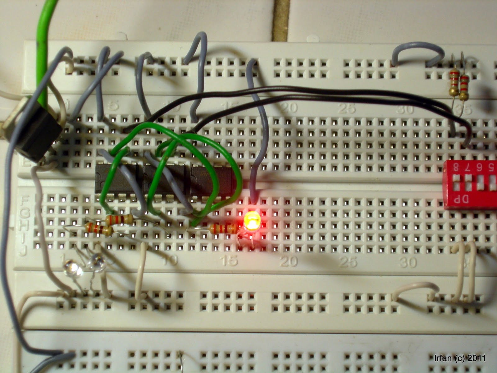
Photographs showing my early experiment of this 555-based NOR gate are shown below:
 |
| The DIP switch is set to give inputs "00". The two powered-on LEDs indicate the output pin (3) of each 555 are both ON, hence the inputs are indeed LOW. The output of the NOR gate is indicated by an LED connected between VCC and an R connected to the GND pin of the right-most 555 (the actual NOR gate output pin). It is currently OFF, indicating that the NOR gate output is HIGH. This gives a correct result as it should be. Inputs "00" gives output "1". |
 |
| The DIP switch is now set to give inputs of "01". The output becomes "0", indicate by the lit LED (current passing through LED, from VCC to 0V of the NOR gate output). |
 |
| Inputs "10" resulting in output "0". |
 |
| Inputs "11" with "0" output. Again, this is correct as a NOR gate. |
A NOR gate as itself may not mean too much. So I decided to think of any possible case study to show the power of this 555-based NOR gate. I need more than just a NOR gate. Digital circuits are either combinational circuits, or sequential systems. And true power of digital systems are in this sequential form, with clocks orchestrating their operation. To make sequential systems, we need memory, or flip-flops. Trying to make use of the internal 555 flip-flop, though seemed very attractive, was another headache that needs to be solved. It became a headache because I wanted the flip-flop to be edge-triggered, and I want the solution to use 555s only. The 555 flip-flop was an SR flip-flop with reset pin, but no clock or enable input. I opened up several textbooks in my posession and good solutions on how to make a flip-flop circuit clock enabled was shown in two of the textbooks I read: Digital Integrated Circuits by Rabaey and Practical Electronics for Inventors by Paul Scherz.
Making a normal D flip-flop to be high level-enabled requires addition of normally two AND gates. Both of these AND gates will require that another signal, the CLOCK signal, be HIGH, in order that any change to the flip-flop output can be made. When the CLOCK signal is LOW, the flip-flop will only see zero inputs on both input terminals, therefore the current state of outputs will be retained.
But the internal circuit of the 555 is unique! Activation of the R and S input of the internal 555 flip-flop requires the opposite logic value of the trigger and threshold input pins of the 555. So unlike a normal SR flip-flop that requires a "00" input for "no change", our 555 will need a "01" input (on the threshold and trigger input pins) to make the internal SR flip-flop do the same "no change" thing. After some contemplation, the solution I came up with looks something like this:
 |
| Making the 555 as a D flip-flop with clock input (high-level active). The 555 will need an AND gate and an OR gate with one input bubble. The AND gate and OR gate could be made with NOR gates, right? |
The AND gate and OR gate (with one bubble input) MUST be made with 555s too for consistency. All ICs in this project are 555-based. To do so, we should transform the above circuit into an equivalent circuit based on NOR and NOT gates. NOT gates can be made simply by connecting the threshold and trigger pins together, forming the input of the inverter. The output of the inverter is also the output pin of the 555, like the sketch below:

To implement the AND and OR gate circuitry mentioned above (for the 555 D flip-flop) using only 555s, we need to build a NOR and NOT-based circuit like this:
 |
| Equivalent circuit of AND and OR gate (with one input bubble) using NOR and NOT gates. NOR and NOT gates will then be implemented using 555s. Therefore this circuit will require 2x3 555s (as NOR gates) and 3x1 555s (as inverters). Total: 9. |
The above solution still needs something more: we need to make the D flip-flop (DFF) edge-triggered instead of level-enabled. One way to do this is to make a master-slave arrangement, using two clock-enabled D flip-flops. If this was to be made entirely with 555s, then it will need one 555 for the SR flip-flop, nine for the clock-enabling thing, and double that for a pair of the same DFF. This gives an astonishing amount of 20 555s, plus one more to invert the clock on one of the DFF. Twenty one 555s is not a small amount of ICs just for a single edge-triggered flip-flop able to keep 1-bit of information only. So I opted to the alternative solution, which was to build a pulse-forming circuit prior to the level-enabled DFF which will turn a clock edge into a very short pulse, like the circuit here (which uses a NOR and an inverter so that it can be built with 555s):
 |
| Short pulse generation from a negative clock edge using a NOR gate (three 555s) and an inverter (one 555). This circuit therefore requires four 555s. |
With this approach, an edge-triggered DFF will need 10+4 or 14 555s. Alternatively, we can use four 556s and six 555s. Single 555s are still necessary in this approach because on our NOR gates, we use one 555 as a resistor with an unordinary use of its ground pin. Fourteen is still a lot, but compared to 20, it's a bit better. Images showing the built DFF can be seen here:

The resulting edge-triggered DFF with the above solution is a negative edge-triggered DFF, with an asynchronous RESET pin (using the RESET pin of the 555). I did not show this in my schematics nor videos, but it is actually built and tested on the 2-bit grey-code counter discussed on my previous post. You can try to zoom the following image of it, where I put a reset button near the LED of Q1. This reset button pulls the reset pin of all 555 DFFs to zero. It worked, but I have no photos or videos yet to show.
 |
| 2-bit synchronous grey-code counter as proof of concept of proposed 555-logic. It works! :D |
A video clip showing my experiment proving that the individual DFF works (as an edge-triggered one) is shown here:
To prove that the 555-logic concept I proposed does really work in a (bit) usefull application, I built a synchronous 2-bit grey code counter implemented entirely in 555-logic. A 555 clock generator was used too, resulting in an equivalent total of 30 555s, already shown above.
btw, ur wife kinda forgot what kind of business that u mentioned..
ReplyDeleteand u're...wow! WOW! :-)